In the past, electricity was the main measure of the economy. Now, computing power will also become another major indicator of the economy.
How is computing power changing the economy? According to IDC’s “2021-2022 Global Computing Power Index Evaluation Report”, for every 1 point increase in the computing power index, the digital economy and GDP will increase by 3.5‰ and 1.8‰ respectively.
Computing power has also attracted the attention of the state. In March 2022, the “Eastern Digital and Western Computing” project was officially launched, that is, by building a new computing power network system integrating data center, cloud computing and big data, the eastern computing power demand will be guided to the west in an orderly manner, and the data center will be optimized. Build a layout to promote synergy between the east and the west.
However, with the advent of the digital age, Moore’s Law has slowed down, and the demand for computing power has grown significantly. The traditional single computing architecture has reached the bottleneck of performance and power consumption.
Entering the era of digital economy, in the face of massive and diverse data, how to break through the bottleneck of computing power, and how to solve the contradiction between how to increase computing power and reduce power consumption? Song Jiqiang, president of Intel China Research Institute, shared Intel’s experience at the CCF Chip conference.
Heterogeneous computing and heterogeneous integration are magic weapons
“Breaking through the bottleneck of computing power is the first step, and solving the calculation effectiveness of diversified data through different methods. Improving computing power while considering the topic of green computing is the second step. It is not possible to solve problems with very energy-intensive computing methods. It is about how to solve the future data processing in an energy-optimized way.” Song Jiqiang said that heterogeneous computing and heterogeneous integration are new approaches to solve these problems, flexible combination of hardware can give full play to the potential of computing power and efficiently handle complex computing load
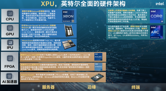
The so-called heterogeneous computing is to use different architectures to process different types of data. To solve problems along this line of thinking, the hardware architecture should not be partial, but should be developed in an all-round way. According to Song Jiqiang, Intel can have different processor architectures for different data, such as CPU, GPU, IPU, FPGA, and AI accelerators, which can be customized for different types of data streams, including different characteristics of data processing.
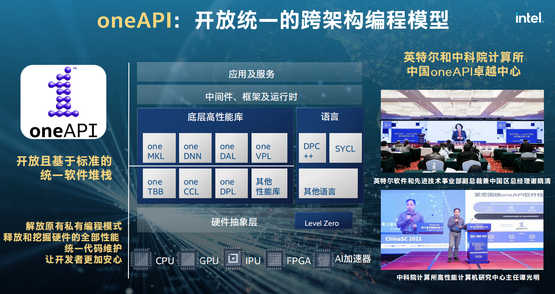
When the hardware is stacked together, someone needs to schedule the hardware and run the program according to the application requirements. At this time, it is the software’s turn to appear, but such a software framework is still relatively scarce. Intel’s oneAPI plays such a role in the market. It only needs to let the user specify the function of the program without specifying which parts run on the CPU, which parts run on the GPU, and which parts run on the AI accelerator. “Through the underlying software function modules and tool chain, the following specific implementations can be distributed on different hardware. When the hardware changes, the following specific implementations also change accordingly, but the above software development code does not need to be changed.”
Do a good job in the chip process and packaging strength to be hard
Of course, for a computing system, three cobblers cannot make up one Zhuge Liang, so this requires each piece of hardware to have extremely strong computing power, and the process and packaging are the keys to achieving computing power.
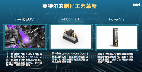
In terms of process, Intel is the first to use the next-generation extreme ultraviolet lithography machine (EUV) based on high numerical aperture, which can further reduce the complexity of the entire process and improve the yield, and can reduce the feature line width of lithography. At the transistor power supply level, Intel will use PowerVia technology at the bottom of the Intel 20A process node to supply power to all upper-layer functional logic components, completely separating the power supply layer from the logic layer, which can use the metal layer more effectively to improve performance.
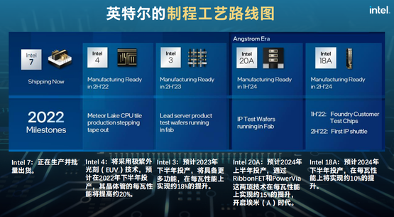
It is worth noting that Intel will have five node evolutions in the next four years. Intel 7 is currently shipping in large quantities, and Intel 4 will be available in the second half of this year. This is the first time Intel has used EUV process nodes; next year, Intel 3 will be mass-produced, and EUV will be used more in the production process; 2024 After mass production of Intel 20A in the first half of the year, it was quickly transferred to Intel 18A in the second half of the year. Song Jiqiang emphasized: “Currently, very good progress has been made in the research and development of Intel 18A and Intel 20A. We feel that these two nodes will be applied to products earlier than expected.”
With all kinds of hardware, a problem faced at this time is how to integrate these hardwares into a system, which requires heterogeneous integration, that is, advanced packaging technology. This process can package chips of different process nodes in a large package, and at the same time take advantage of the size, bandwidth, and power consumption brought by advanced packaging, so that they do not have as much delay and bandwidth as the original board-level packaging. reduce.
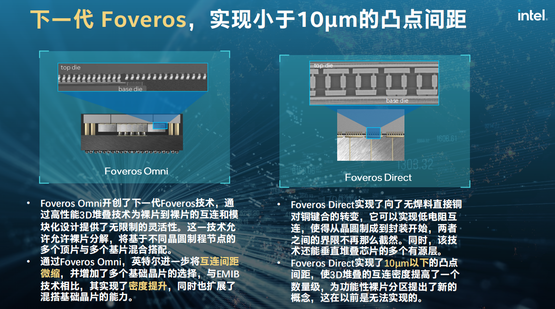
Currently, Intel has two technologies that enable heterogeneous integration, one is EMIB (Embedded Multi-Chip Interconnect Bridge), which is a 2.5D packaging technology that can The bump pitch between them is reduced to less than 50 microns, and it may be reduced to the level of 45 microns and 30 microns in the future; the other is Foveros, which is a 3D packaging technology that can integrate different computing chips on a vertical level. Packaging, the pitch of package bumps can be reduced to 36 microns, and it can continue to be reduced to 20 microns in the future, or even below 10 microns.
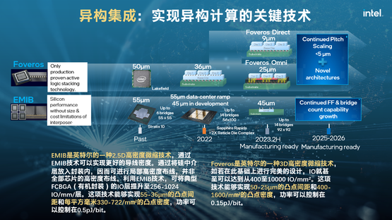
Foveros Omni and Foveros Direct are two technologies that Intel will use in 3D packaging in the future. The former can use a common method to shrink the contact point spacing between different chips to 25 microns, and can also directly use copper pillars for the upper chip. Power supply, which has a density improvement of nearly 4 times compared with EMIB; the latter is a more advanced technology that does not require solder and directly allows copper-to-copper bonding, which can achieve lower resistance interconnects. This way The pitch between bumps can be further reduced to less than 10 microns.
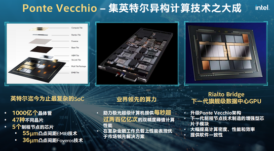
So are there any products that are heterogeneously integrated? Song Jiqiang showed a very typical example – Ponte Vecchio. It is Intel’s most complex SoC in the field of high-performance computing GPUs. This SoC uses a total of 47 different chips on 5 different process nodes, some from Intel and some from TSMC. In addition, they are packaged with EMIB technology at the horizontal level and integrated with Foveros technology at the vertical level.
This construction creates a computing system designed for high-performance computers, including a Xeon processor and a specialized Xe-based Ponte Vecchio GPU, currently used in the Aurora supercomputer. The next-generation flagship data center GPU will be code-named Rialto Bridge, and its internal chiplets will use a newer process node and will also use the latest packaging technology.
More powerful next-generation computing
To make the computing power more powerful, in addition to using the existing paradigm, it also requires a new computing model. Neuromorphic computing and quantum computing are the secret weapons that can drastically reduce power consumption by 1,000 times or increase computing power by 1,000 times.
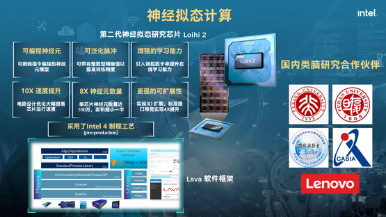
The great advantage of neuromorphic computing is that it can completely break through the current mode of providing computing power by means of stack-multiply-adders at the algorithm level and hardware structure design level, but to simulate the form of human neurons to construct the underlying layer. Calculation unit, and most of them are integrated storage and calculation. This chip is constructed, and then programmed through a spiking neural network to implement artificial intelligence algorithms. Computation with neuromorphic consumes more than a thousand times less energy compared to conventional CPUs or GPUs, so it’s very noteworthy.
Intel’s Loihi is a representative experimental chip for neuromorphic computing, and it is now in its second generation. Loihi 2 is based on Intel 4 process technology, which is 10 times faster than the previous generation, the number of neurons in a single chip is increased by 8 times, and the area is reduced by half. Specifically, Loihi 2 can have up to 1 million neurons on a single chip. Intel had previously integrated 768 Loihi neuromorphic chips into five standard server-sized chassis into a data center rack-mounted system, Pohoiki Springs, with a staggering 100 million neurons. In addition, Intel also proposed a complete open source Lava software framework to deal with the software problems of neuromorphic computing.
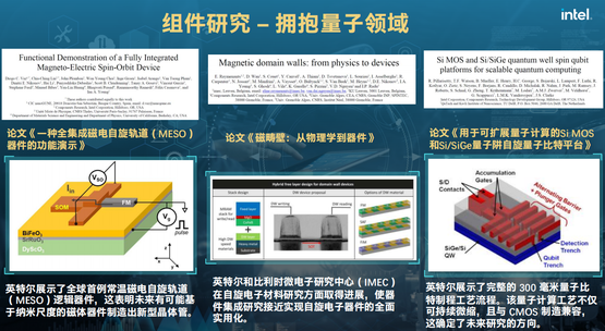
Intel’s continuous research on quantum computing includes two aspects of research.
On the one hand, it is a new device that applies quantum physical effects to traditional computing and traditional storage: using magnetoelectricity and electron spin orbits, the two devices are well combined to construct MESO logic devices, a breakthrough in this technology. The point is to apply spintronic devices, which are mostly used for storage, in logic computing; through the production process, Intel has made practical experiments on the concept of magnetic domains at the level of electronic devices, and the tests have achieved good results. It is very important to do storage.
On the other hand is large-scale quantum computing: qubits are constructed using technologies based on silicon or silicon germanium devices that are very compatible with Intel’s current silicon-based production processes. These qubits are constructed using quantum well technology to construct the electron spins of the silicon inside. , by controlling the direction of the spin, it becomes a qubit, which can be combined to do large-scale quantum computing.
Research to support computing power
“Component research has always been a very important research task for Intel’s production, manufacturing, and R&D departments, and it is also very active in the entire semiconductor R&D academic circle.” Song Jiqiang said.
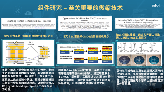
Hybrid bonding technology is closely related to Foveros Direct, which studies how to directly bond between copper and copper without solder joints, and can achieve very high interconnection density technology. This technology involves how the industry can package chips from different manufacturers well in the future, so new industry standards and testing procedures are needed. Song Jiqiang said: “Because the contact points of chip interconnection are so dense and small, new test methods and test requirements need to be re-formulated, which are very different from before, and a new ecosystem needs to be established.”
The research on 3D stacking of CMOS transistors is a technology closely related to RibbonFET, which can achieve 30%~50% shrinkage by stacking CMOS transistors. How to choose new materials to make contact layers and construct some channels is very important, which may further improve the performance of transistors.
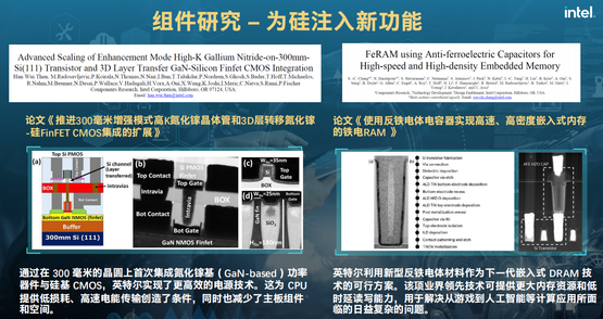
On the basis of silicon CMOS, new transistor materials and structures can be further superimposed to inject new functions into silicon transistors. Power management technologies including enhancement-mode high-K GaN transistors and silicon FinFET transistors combined, process antiferroelectric materials for next-generation embedded memory technologies.
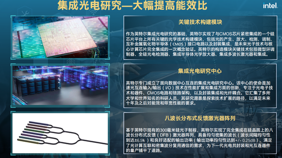
Optoelectronics is a continuous concern of the academic community, and Intel also has a lot of layout and progress in integrated optoelectronics. The problem of high bandwidth and low energy consumption in light communication occurs because the photoelectric conversion efficiency is not high, and the short distance is not as cost-effective as the long distance. Intel realizes the integration of all key modules on one platform. Photoemission, amplification, detection, and modulation can all be fabricated in a large chip module using CMOS technology, and the overall size and power consumption are greatly reduced. At the same time, it also involves some basic device-level innovations. Intel has developed an 8-wavelength laser array on a silicon wafer. This is a light-generating component, which will greatly improve the accuracy and energy efficiency of optoelectronic packaging. Great help and pave the way for mass production of optoelectronic co-packages and optical interconnect devices.
Summarize
Intel’s research covers not only computing in a few years, but also advanced computing technologies that will lead the future. “From heterogeneous computing, heterogeneous integration, to device-level innovation, to new energy-efficient architecture technologies and innovations in optical interconnect technology, these are all to promote the development of the green computing field. Together we can put computing power It can be increased by a thousand times, but the sustainable development of the entire earth’s ecology can still be maintained.” Song Jiqiang said.
Text/Fu Bin
This article is reproduced from: http://www.guokr.com/article/461966/
This site is for inclusion only, and the copyright belongs to the original author.