Recently, 36氪 was informed that Shenzhen Taiyan Semiconductor Equipment Co., Ltd. (hereinafter referred to as “Taiyan Semiconductor”) received tens of millions of yuan in Series A financing from Hechuang Capital. This round of funds will be mainly used for product expansion and delivery.
Taiyan Semiconductor is a semiconductor process and equipment service provider in the field of advanced packaging. It can provide customers with advanced packaging production lines such as SiP, Fanout, Chiplet, 3D, etc. Laser (laser) + Plasma (plasma) + Sputter (coating) complete composite process and Process application equipment.
Under the situation that Sino-US trade is stuck, the Chinese government strongly supports the development of localization of semiconductor equipment. With the help of policies and capital, the upsurge of semiconductor manufacturers to build factories, and the large-scale expansion of local foundry and storage IDM, promote the expansion of the equipment market. The continuous growth of China’s semiconductor equipment market and the acceleration of the domestic substitution trend have provided huge development space for Chinese semiconductor equipment manufacturers. According to SEMI data, global sales of semiconductor equipment in 2021 will increase by 45% year-on-year to $103 billion, a record high.
The traditional packaging equipment market is mainly dominated by companies from the United States, Japan and South Korea. China still has suppliers with good cost performance in the equipment supply of some semiconductor process nodes, but in the fields of high-end technology and advanced technology, China’s semiconductor equipment supply capacity is slightly insufficient. . In the field of semiconductor packaging, advanced packaging technology is different from traditional packaging technology. Advanced packaging is in its infancy at home and abroad. For China, semiconductor equipment for advanced packaging has the potential for rapid development.
As semiconductor processes get closer and closer to physical limits, the industry has begun to explore the use of advanced packaging to improve product performance and improve product processes. According to the 2020 report of the CSIA Packaging Branch, the localization rate of domestic advanced packaging production line equipment is as high as 20%-50%, and the localization rate is generally higher than that of traditional packaging production lines.
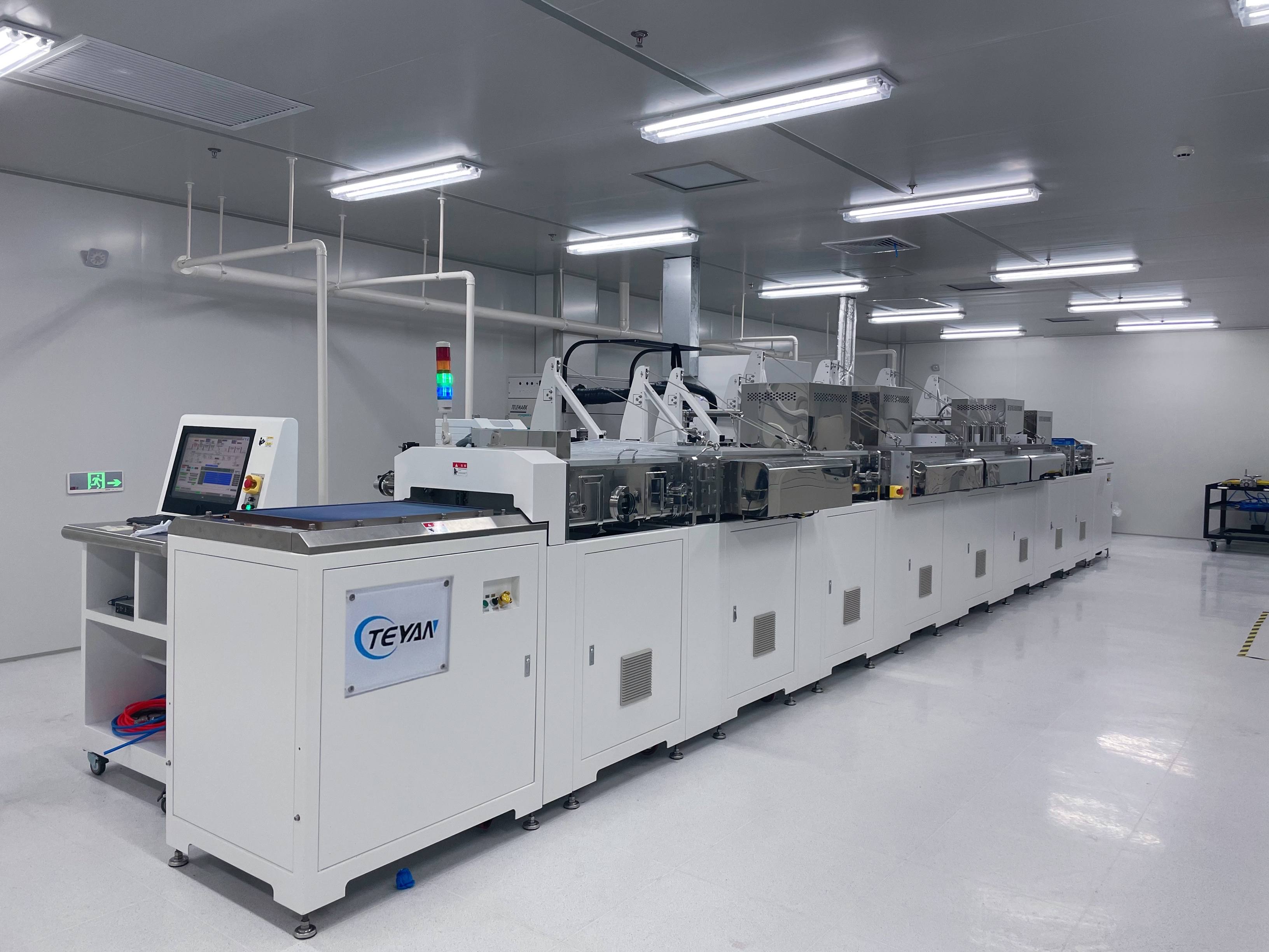
At present, Taiyan Semiconductor has three types of packaging equipment: sputtering equipment, laser equipment, and plasma equipment.
- Sputtering equipment: It has great advantages in the production of large-size products, and can realize functions such as heat dissipation, RDL, and EMI through the coating process. Taiyan has core design capabilities and mass production processes in independently developed cavity independent refrigeration systems, high heat dissipation systems, plasma pretreatment systems, etc. With these core capabilities, Taiyan’s sputtering equipment can achieve EMI functions when implementing EMI functions. The industry-leading superb level, specifically, its sidewall coverage can reach more than 70%, while the industry index is generally around 40%.
- Laser equipment: It can provide customers with services such as chip surface laser coding/reading, chip cutting and grooving, 3D packaging laser drilling, etc. Taiyan’s laser equipment integrates marking and AOI detection, and is compatible with SECS GEM (SEMI connectivity standard) E30, can be used for equipment communication and control) and RMS (semiconductor packaging and testing equipment RMS system), can provide its own IP marking, detection, control integration software, and through innovative optical path design to ensure high precision and high stability.
- Plasma equipment: It has the functions of substrate and wafer plasma cleaning, photoresist slag cleaning, RDL circuit etching, RMC dry etching thinning, WPC plasma wafer cutting, etc. The thinning process of this equipment can achieve a very high degree of warpage. Small, can enhance the safety and reliability of the package.
Sputter sputtering equipment
Semiconductor production equipment directly affects the final quality of semiconductor products and is the core and most important factor in the entire production process. Downstream packaging factories, considering the stability and continuity of their own production, are more inclined to choose suppliers with a certain production scale and popularity. Therefore, for early semiconductor equipment suppliers, the barriers to entry to downstream customers are very high.
A lot of industry knowledge and accumulation are needed behind the various subtle links of semiconductor equipment, from the design of product parts to how the direction of the automatic feeding system matches other products on the production line. Zhang Shaobo, founder of Taiyan, said, “In the field of laser marking, there are many domestic competitors, but there are few equipment companies that can sell to top international semiconductor companies, and Taiyan is one of them.”
Taiyan’s equipment has passed the strict certification of international customers, including European industrial vehicle chip giants, and meets the requirements of technical specifications. The product performance and quality have reached the international leading level. The research has successfully broken the downstream access barriers in the semiconductor equipment industry.
In addition, compared with traditional semiconductor equipment suppliers that only focus on certain types of semiconductor equipment, Taiyan can provide downstream customers with the planning of a complete set of equipment for advanced packaging production lines, helping customers reduce product matching processes. This capability of Taiyan is due to its excellent process design capabilities and deep accumulation in the industry. At present, Taiyan has carried out this program planning business in a number of packaging factories with advanced packaging technology.
Taiyan Semiconductor currently has a 1,500-square-meter factory and is expected to start mass production after this round of financing.
Dr. Liu Huarui, vice president of Hechuang Capital, said that the industry generally believes that advanced packaging is the path to continue to improve the functional performance of the chip after the current semiconductor manufacturing process reaches the physical limit. As a solid upstream supporting the development of the domestic advanced packaging industry, Taiyan Semiconductor’s equipment product system Complete, covering multiple segments of the advanced packaging industry, the Taiyan team has outstanding advanced packaging process design capabilities, can give full play to its own advantages, and contribute more to the development of the domestic semiconductor equipment industry and the implementation of the domestic substitution strategy.
media coverage
36Kr investment community start-up state
Related events
- Taiyan Semiconductor completed tens of millions of yuan in Series A financing, and Hechuang Capital made exclusive investment2022-04-28
- Xinyuan Semiconductor completes nearly $100 million in Pre-A round financing2021-04-06
This article is reprinted from: https://readhub.cn/topic/8fzFFi3fso3
This site is for inclusion only, and the copyright belongs to the original author.